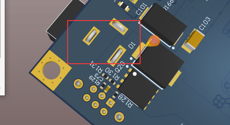
You can observe that there are many large and small holes in the circuit board. You will find that there are many dense small holes, and each hole is designed with its purpose. These holes can be divided into two types: PTH (Plating Through Hole, electroplating pores) and NPTH (non -electroplatern holes). Here One side runs through the other side. In fact, in addition to the hole in the circuit board, there are other holes that are not running through the circuit board.
PCB noun explanation: pass through, blind holes, buried holes.
1. How to distinguish the two types of pores of PTH and NPTH?
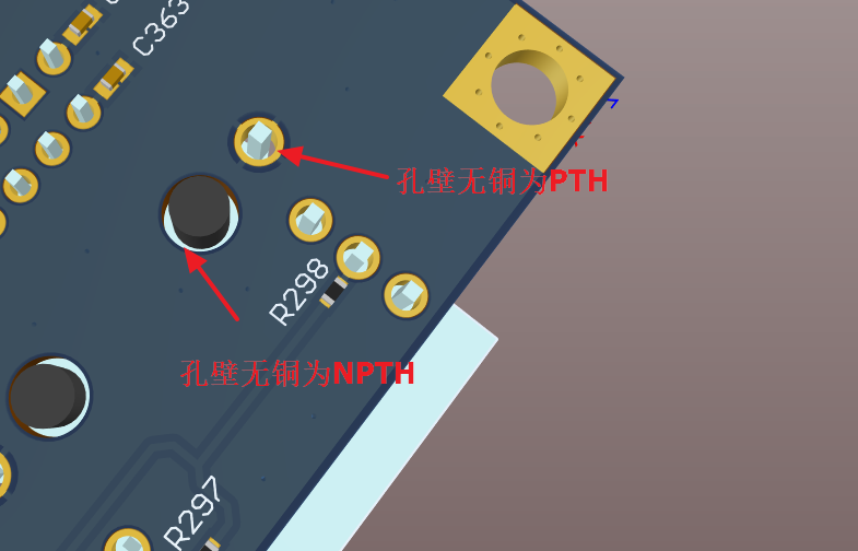
See if there are bright plating marks on the hole wall, you can judge. The holes with electroplating marks are PTH, and holes without electroplating marks are NPTH. As shown below:

2. What is the use of NPTH?
It is found that the aperture of NPTH is usually larger than PTH, because most of the NPTH is used for lock screws, and some are used to install some connected connectors to fix them. In addition, some will be used as a positioning of testing tools on the edge of the board.
3. What is PTH? And what is Via?
Generally, there are two uses of PTH holes in the circuit board. One is used to weld the traditional DIP parts. The aperture of these holes must be larger than the diameter of the welding foot of the part, so that the parts can be inserted into the hole.

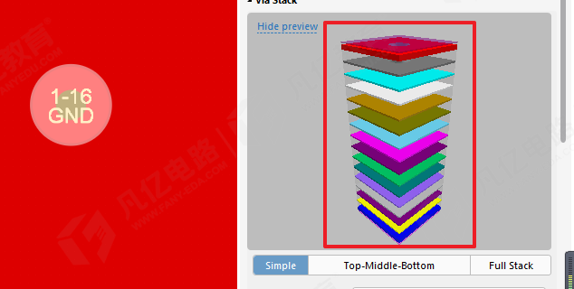
Another relatively small PTH is usually called VIA. It is used for two or multi -layers between two or multi -layers used to connect and guide the circuit board (PCB). Many copper foil layers are piled up and accumulated. Each layer of copper foil (Copper) will be paved with another layer of insulating layer, which means that the copper foil layer cannot be communicated with each other. That's why it is called "Ditto". Via does not see the existence of holes from outside. Because the purpose of VIA is to turn on the copper foil of different layers, the electrophilic is needed to be turned on, so VIA is also a kind of PTH.

 Meizhou Ruiputuo Technology Co.,Ltd