 Meizhou Ruiputuo Technology Co.,Ltd
 The calculation of PCB current carrying capacity has always lacked authoritative technical methods and formulas. Experienced CAD engineers can make more accurate judgments relying on personal experience. But for CAD novices, it is not a difficult problem.
For high-current power supply traces, if the trace width is not evaluated in the correct way, it may cause excessive current and burn the board traces; for high-speed signals, if the trace width is not calculated properly, it may cause impedance mismatch. cause signal integrity problems.
2. What factors are related to PCB routing
The routing of PCB is mainly related to the current magnitude, temperature rise, which layer the routing is on, and copper thickness.
Not much to say, for engineering, the most important thing is application. Of course, some data will be posted on the website, as follows:

The purpose of this article is to recommend a website for calculating the line width of PCB traces, as follows:

The yellow area is the information we need to input, including the current size, copper thickness, temperature rise, the remaining ambient temperature and the length of the trace have little effect on the trace width, mainly affecting the voltage drop and loss. We use this website to verify the data given by other websites. Taking copper thickness 35um (1OZ), current 0.55A, and allowable temperature rise of 10° as an example, the data given is that the line width is 0.2mm, and we perform input calculations ,As follows:
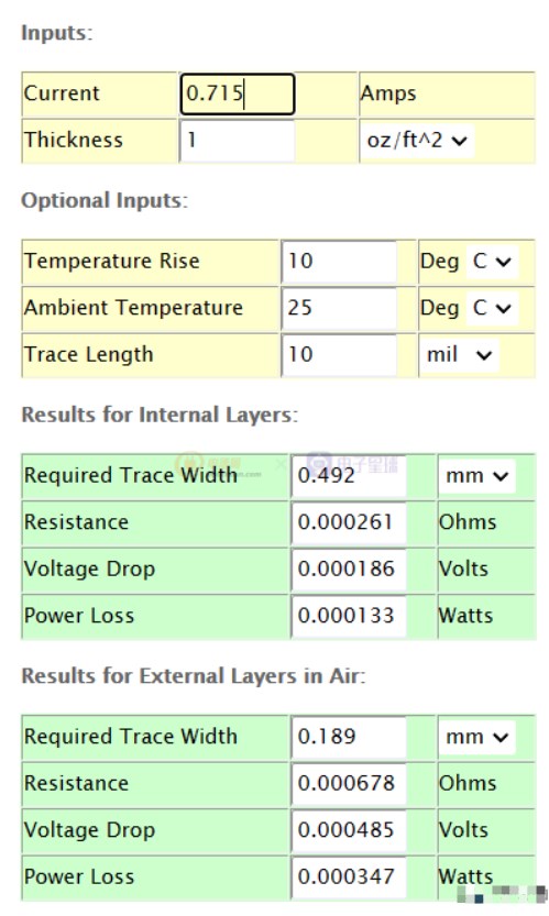
The outer layer line width is 0.189mm, and the inner layer line width is 0.492. Using this software, the current needs to be multiplied by 1.3 times the input (with a certain margin), 1.3*0.55=0.715, and the outer layer line width is obtained It is close to 0.2mm in the table. What needs special attention here is that for many engineers, the line width of the outer layer is not the same value as the line width of the inner layer.