Explaining Laser Direct Imaging in PCB Fabrication by rpttechpcb
when it comes to a prototype circuit board, PCB layout is one of the most important aspects. taking into account the smallest things goes wrong, the entire board will be damaged and it will not function appropriately, so PCB layout is extremely important. The imaging process, one of the most important steps in the PCB assembly process, and it does well in creating the PCB pattern.
For engineers, laser direct imaging ( LDI ) can make a good effect on creating an imaging pattern on laminates in a streamlined process. The laminates of a PCB are fabricated by curing with thermosetting resin under the pressure and temperature layers of cloth or paper to form an integral final piece of uniform thickness. Now rpttechpcb will explain about laser direct imaging ( LDI ) for flexible circuits.
What is laser direct imaging ( LDI )?
When fabricating a circuit board, the circuit traces are defined by what is the imaging process. Laser direct imaging ( LDI ) exposes the traces directly with a highly focused laser beam that in NC controlled, instead of flooded light passing through a photo tool, a laser beam will digitally create the image.
How does laser direct imaging ( LDI ) work?
Laser direct imaging needs a PCB with the photo-sensitive surface that is positioned under a computer controlled laser. And then the computer is creating the image on the board with the light of laser. A computer scans the board surface into a raster image, matching the raster image to a pre-loaded CAD or CAM design file that includes the specifications for the necessary image intended for the board, the laser is used for directly creating the image on the board.
Now it will be a matter of updating the design file as changing to the necessary image, which can be done more cost-effectively and consistently than traditional photo ways.
The laser direct image process typically goes as follows:
1. Coat resist on the copper laminate;
2. Exposing the photo of the PCB pattern on the resist;
3. Develop the unexposed resist;
4. Etch the exposed copper.
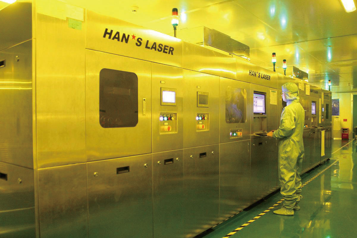
Advantages of LDI over photo processing
When creating the photo tool for generating the image on the board, it needs to have multiple steps for the traditional photo processes. For years, there are a lot of challenges for the PCB manufacturer. And LDI have a lot of advantages:
Quality - in the past, the problem of photo films have led to imperfect images because of inherent susceptibility to fluctuations in temperate or humidity. Laser images bring about more accurate and consistent images, and clear up any film-related defects.
There have accurate positioning and improved resolution. As well as more precise image lines, spaces, and image alignment.
When the photo method is providing the most accurate transfer of images to the boards, it needs to have temperature and humidity controlled environments. LDI reduces the effect of environment on the resulting images, and eliminates the impacts of light refraction inherent with photo processing techniques.
LDI manufacturing has particular advantages under the circumstances of short runs or quick turn-around, and it’s impractical for the creation of artwork and setup of photo tool methods. When it comes to tight registration and close tolerances, LDI is also an important factor.
Nowadays, taking photo technology as a practical tool in creating PCB images because the customers have the demands for smaller, lighter, high-density PCBs.
If you have any question , please feel free to contact me sales@rpttechpcb.com
 Meizhou Ruiputuo Technology Co.,Ltd