 Meizhou Ruiputuo Technology Co.,Ltd
 During the PCB design process, the division of the power plane or the segmentation of the horizon will cause the plane incompleteness. In this way, when the signal wiring, its reference plane will appear from one power to another. This phenomenon is called a signal split.
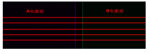
跨分割现象示意图
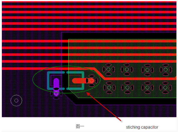
Cross -segmentation may have nothing to do with low -speed signals, but in high -speed digital signal systems, high -speed signals use reference plane as the return path, which is the return path. When the reference plane is incomplete, the following adverse effects will occur: A. The impedance of the wiring will be discontinuous; b. The circulation area of the current and increase the electromosomium of the circuit, making the output waveform easily oscillate; E. Increases radiation interference to space, and is easily affected by the space magnetic field; f. Increase the magnetic field coupling with other circuits on the board to generate a magnetic field coupling Possibilities; G and ring circuit inductances constitute a common modular radiation source, and co -mode radiation is generated through external cables. Therefore, the PCB wiring should be as close to one plane as much as possible and avoid cross -segmentation. If you have to split or close to the plane of the power area, these situations are only allowed to exist in low -speed signal lines. If the processing of splitting in the PCB design is inevitable in the PCB design, what should be dealt with? In this case, it is necessary to sewn the division to provide a shorter return pathway for the signal. The common processing methods include adding a sewing capacitor and a cross -line bridge. 1. Stiching Capacitor is usually placed with a 0402 or 0603 porcelain capacitance at the signal split. The capacitor's capacity is 0.01UF or 0.1 UF. At the same time, try to ensure that the signal cable is within the range of the stitching capacitance 200mil, the smaller the distance, the better; the network of the network on both ends of the capacitor corresponds to the reference plane network, see the network connected to both ends of the capacitor in the figure below. The two colors are high high. Two different networks of bright:
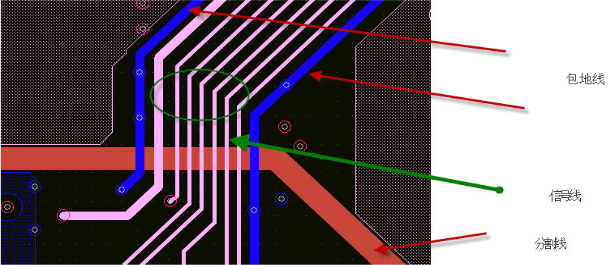
2. The common part of cross -line bridge is the signal "package processing" on the signal layer on the signal layer. It may also include the signal line of other networks. This "package land" line is as thick as possible. Essence
知识扩展:高速信号布线技巧
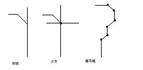
1. Multi -layer wiring high -speed signal wiring circuits are often highly integrated and the wiring density is large. The use of multi -layer boards is both necessary for wiring and an effective means to reduce interference. Reasonable selection of the number of layers can greatly reduce the size of the printing plate, can make full use of the middle layer to set the shield, can better achieve the nearby ground, can effectively reduce the parasitic inductance, can effectively shorten the transmission length of the signal, greatly reduce the signal to greatly reduce the signal Cross interference in the middle. Buy components in stock. 2. The less the lead bending, the better, the less high -speed circuit device's tube feet, the less the bending of the tube. The leader of the high -speed signal wiring circuit wiring is best to adopt a full line, which needs to be turned. You can use a 45 ° folding line or an arc to turn. One requirement can reduce the transmission of high -speed signals and coupling between each other, and reduce the radiation and reflection of the signal. 3. The shorter the lead, the better the high -speed signal wiring circuit device's feet. The longer the lead, the greater the distributed inductance and distributed capacitor value brought about. It has a lot of impact on the passing of the high -frequency signal of the system. At the same time, it will also change the characteristics of the circuit, which will cause the system to reflect and oscillate. 4. The less alternating between the lead layer, the better the high -speed circuit device's feet. The so -called "less inter -layer of the lead, the better," refers to the less holes used during the component connection process, the better. It is reported that an over -holes can bring about 0.5PF distributed capacitors, which causes the delay of the circuit to increase significantly, and reducing the number of over -holes can significantly increase the speed. 5. Pay attention to parallel cross interference interference between the tube of the high -speed circuit device, the less, the better. The so -called "less inter -layer of the lead, the better," refers to the less holes used during the component connection process, the better. It is reported that an over -holes can bring about 0.5PF distributed capacitors, which causes the delay of the circuit to increase significantly, and reducing the number of over -holes can significantly increase the speed. 6. Pay attention to parallel cross -dry high -speed signal wiring. Pay attention to the "cross interference" introduced by the close -range parallel line of the signal line. If the parallel distribution cannot be avoided, a large area of "ground" can be arranged on the reverse area of the parallel signal line to significantly reduce interference interference. Essence 7. Avoid branches and stump high -speed signal wiring should avoid branches or form stumps (STUB) as much as possible. The stump resistance has a great impact, which can lead to the reflection and overwhelming of the signal, so we usually avoid tree stumps and branches when designing. The chrysanthemum chain is used to reduce the impact on the signal.
8. The signal line is as much as possible in the inner layer of high -frequency signal lines. It is easy to generate larger electromagnetic radiation at the surface, and it is also vulnerable to external electromagnetic radiation or factors. The high -frequency signal line is between the power supply and the ground line. The radiation generated by the absorption of electromagnetic waves through the power supply and the underlying layer will be reduced a lot.