 Meizhou Ruiputuo Technology Co.,Ltd
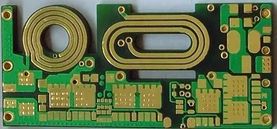
An increasing number of power electronics products are taking advantage of a growing trend in the printed circuit board industry: Heavy Copper and EXTREME Copper Printed Circuit Boards.
Most commercially available PCBs are manufactured for low-voltage/low power applications, with copper traces/planes made up of copper weights ranging from 1/2 oz/ft2 to 3 oz/ft2. A heavy copper circuit is manufactured with copper weights anywhere between 4 oz/ft2 to 20 oz/ft2. Copper weights above 20 oz/ft2 and up to 200 oz/ft2 are also possible and are referred to as EXTREME Copper. Our discussion will focus primarily on Heavy Copper.
The construction of a heavy copper circuit endows a board with benefits such as:
Increased endurance to thermal strains.
Increased current carrying capacity.
Increased mechanical strength at connector sites and in PTH holes.
Use of exotic materials to their full potential (i.e., high temperature) without circuit failure.
Reduced product size by incorporating multiple copper weights on the same layer of circuitry (see Figure 1).
Heavy copper plated vias carry higher current through the board and help to transfer heat to an external heatsink.
On-board heatsinks directly plated onto the board surface using up to 120-oz copper planes.
On-board high-power-density planar transformers

Figure 1. Sample featuring 2oz, 10oz, 20oz, and 30oz copper features on the same layer.
Heavy Copper Circuit Construction
Standard printed circuit boards, whether double-sided or multilayer, are manufactured using a combination of copper etching and plating processes. Circuit layers start as thin sheets of copper foil (generally 0.5 oz/ft2 to 2 oz/ft2) that are etched to remove unwanted copper, and plated to add copper thickness to planes, traces, pads and plated-through-holes. All of the circuit layers are laminated into a complete package using an epoxy-based substrate, such as FR4 or polyimide.
Boards incorporating heavy copper circuits are produced in exactly the same way, albeit with specialized etching and plating techniques, such as high-speed/step plating and differential etching. Historically, heavy copper features were formed entirely by etching thick copper clad laminated board material, causing uneven trace sidewalls and unacceptable undercutting. Advances in plating technology have allowed heavy copper features to be formed with a combination of plating and etching, resulting in straight sidewalls and negligible undercut.
Plating of a heavy copper circuit enables the board fabricator to increase the amount of copper thickness in plated holes and via sidewalls. It's now possible to mix heavy copper with standard features on a single board, also known as PowerLink. Advantages include reduced layer count, low impedance power distribution, smaller footprints and potential cost savings. Normally, high-current/high-power circuits and their control circuits were produced separately on separate boards. Heavy copper plating makes it possible to integrate high-current circuits and control circuits to realize a highly dense yet simple board structure.
The heavy copper features can be seamlessly connected to standard circuits. Heavy copper and standard features can be placed with minimal restriction provided the designer and fabricator discuss manufacturing tolerances and abilities prior to final design (Figure 2).

Figure 2. 2oz features connect control circuits while 20oz features carry high current loads.
Current Carrying Capacity and Temperature Rise
The amount of current a copper circuit can safely carry depends on how much heat rise a project can withstand, since heat rise and current flow are related. When current flows along a trace, there is an I2R (power loss) that results in localized heating. The trace cools by conduction (into neighboring materials) and convection (into the environment). Therefore, to find the maximum current a trace can safely carry, we must find a way to estimate the heat rise associated with the applied current. An ideal situation would be to reach a stable operating temperature where the rate of heating equals the rate of cooling. An IPC formula can be used to model this event.
| Track Width (inch) | ||||||||||
|---|---|---|---|---|---|---|---|---|---|---|
| Cu weight (oz/ft2) | Thickness (inch) | 0.0625 | 0.1250 | 0.2500 | 0.5000 | 1.0000 | 2.0000 | 4.0000 | 8.0000 | 16.0000 |
| 1 | 0.0014 | 4.6 | 7.6 | 12.5 | 20.7 | 34.2 | 56.6 | 93.6 | 154.7 | 255.6 |
| 2 | 0.0028 | 7.6 | 12.5 | 20.7 | 34.2 | 56.6 | 93.6 | 154.7 | 255.6 | 422.5 |
| 4 | 0.0056 | 12.5 | 20.7 | 34.2 | 56.6 | 93.6 | 154.7 | 255.6 | 422.5 | 698.4 |
| 6 | 0.0084 | 16.8 | 27.8 | 46.0 | 76.0 | 125.5 | 207.5 | 343.0 | 566.9 | 937.1 |
| 8 | 0.0112 | 20.7 | 34.2 | 56.6 | 93.6 | 154.7 | 255.6 | 422.5 | 698.4 | 1154.4 |
| 10 | 0.0140 | 24.4 | 40.3 | 66.5 | 110.0 | 181.8 | 300.5 | 496.7 | 821.1 | 1357.1 |
| 12 | 0.0168 | 27.8 | 46.0 | 76.0 | 125.5 | 207.5 | 343.0 | 566.9 | 937.1 | 1548.9 |
| 14 | 0.0196 | 31.1 | 51.4 | 84.9 | 140.4 | 232.0 | 383.6 | 634.0 | 1047.9 | 1732.1 |
| 16 | 0.0224 | 34.2 | 56.6 | 93.6 | 154.7 | 255.6 | 422.5 | 698.4 | 1154.4 | 1908.1 |
| 18 | 0.0252 | 37.3 | 61.7 | 101.9 | 168.4 | 278.4 | 460.2 | 760.7 | 1257.3 | 2078.2 |
| 20 | 0.0280 | 40.3 | 66.5 | 110.0 | 181.8 | 300.5 | 496.7 | 821.1 | 1357.1 | 2243.2 |
| 24 | 0.0336 | 46.0 | 76.0 | 125.5 | 207.5 | 343.0 | 343.0 | 937.1 | 1548.9 | 2560.2 |
| 28 | 0.0392 | 51.4 | 84.9 | 140.4 | 232.0 | 383.6 | 634.0 | 1047.9 | 1732.1 | 2863.0 |
| 32 | 0.0448 | 56.6 | 93.6 | 154.7 | 255.6 | 422.5 | 698.4 | 1154.4 | 1908.1 | 3154.0 |
| 36 | 0.0504 | 61.7 | 101.9 | 168.4 | 278.4 | 460.2 | 760.7 | 1257.3 | 2078.2 | 3435.1 |
| 40 | 0.0560 | 66.5 | 110.0 | 181.8 | 300.5 | 496.7 | 821.1 | 1357.1 | 2243.2 | 3707.8 |
| 45 | 0.0630 | 72.5 | 119.8 | 198.0 | 327.3 | 541.0 | 894.3 | 1478.1 | 2443.2 | 4038.3 |
| 50 | 0.0700 | 78.2 | 129.3 | 213.7 | 353.3 | 584.0 | 965.2 | 1595.5 | 2637.1 | 4358.9 |
| 55 | 0.0770 | 83.8 | 138.6 | 229.0 | 378.6 | 625.7 | 1034.3 | 1709.6 | 2825.8 | 4670.8 |
| 60 | 0.0840 | 147.6 | 244.0 | 403.2 | 666.5 | 1101.7 | 1820.9 | 3009.8 | 4974.9 | |
| 70 | 0.0980 | 165.0 | 272.8 | 450.9 | 745.3 | 1231.9 | 2036.2 | 3365.7 | 5563.1 | |
| 80 | 0.1120 |
PCB product:4-26 layer board matelial:FR4 TG170 ,TG150 Material brand:KB,shengyi,taconic,rogers,MEGTRON6,MEGTRON7,Isola copper thick:1OZ,2OZ.3OZ.4OZ.5OZ Surface Treatment:ENIG,HASL, OSP,Goldfinger,immersion silver pcb thickness:1.6MM low-cost PCB,Cheap PCB, Low price for PCB,94V0 PCB solder mask:green,red,biue,white,black Silk-Screen:wihte,black,yellowMin Line Width/Space:3/3mil,4/4mil. If you have any question , please feel free to contact me sales@rpttechpcb.com
PREVIOUS:LED SMT Assembly NEXT:12 layer pcb Related Products | ||||||||


