 Meizhou Ruiputuo Technology Co.,Ltd
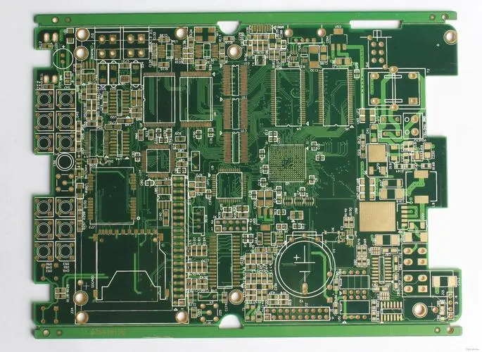
Generally speaking, a four-layer industrial control mother circuit board can be divided into a top layer, a bottom layer, and two middle layers. The top layer and the bottom layer take the signal line, and the middle layer first uses the ADD PLANE command DESIGN/LAYER STACK MANAGER to add INTERNAL PLANE1 and INTERNAL PLANE2 respectively as the most used power layer such as VCC and ground layer such as GND (that is, connect the corresponding network label. Note Do not use ADD LAYER, this will increase MIDPLAYER, the latter is mainly used for multi-layer signal line placement), so PLNNE1 and PLANE2 are two layers of copper that connect the power supply VCC and ground GND. If there are multiple power sources such as VCC2, etc. or ground layers such as GND2, etc., first use a thicker wire or fill FILL in PLANE1 or PLANE2 (at this time, the copper corresponding to the wire or FILL does not exist, and the wire or FILL can be clearly seen when facing the light. fill) to delineate the general area of the power supply or ground (mainly for the convenience of the PLACE/SPLIT PLANE command later), and then use PLACE/SPLIT PLANE to delineate the area in the corresponding areas of INTERNAL PLANE1 and INTERNAL PLANE2 (that is, VCC2 copper and GND2 copper sheet, there is no VCC in this area in the same PLANE) range (note that different network layers in the same PLANE should not overlap as much as possible. Let SPLIT1 and SPLIT2 overlap two pieces in the same PLANE, and SPLIT2 is inside SPLIT1, plate making It will automatically separate the two pieces according to the border of SPLIT2 (SPLIT1 is distributed on the periphery of SPLIT). Just pay attention to the pads or vias in the same network table as SPLIT1 when overlapping, and do not try to connect to SPLIT1 in the area of SPLIT2, and there will be no failure. question). At this time, the vias in this area are automatically connected to the corresponding copper skin of this layer, and the device pins such as DIP packaged devices and connectors passing through the upper and lower boards will automatically get out of the way of the PLANE in this area. Click DESIGN/SPLIT PLANES to view each SPLIT PLANES.
3 Quality assurance of PCB multilayer board
The quality assurance of PCB multilayer boards is defined in IPC. The surface process is anti-oxidation. If the vacuum packaging is not removed, it will be used within half a year. If the vacuum packaging is removed, it will be used within 24 hours, and the temperature and humidity are controlled. Under the environment, the board should be used within one year without opening the package, and the film should be pasted within one hour after opening. The temperature and humidity should also be controlled. The gold board is the same as the tin board, but the control process is stricter than that of the tin board.
4 PCB multilayer board parameters
Substrate / Thickness : FR-4/1.2mm
Size: 140mm*159mm
Minimum Line Width/Space: 6mil/6mil
Minimum aperture: 0.4mm
Surface Treatment : Electroplated Gold
File Format: gerber
Category : For computer; Four-ply
Substrate / Thickness : FR-4/1.6mm
Size: 294mm*200mm
Minimum Line Width/Space: 5mil/5mil
Minimum aperture: 0.3mm
Surface treatment: HASL (hot air leveling)
5 Necessary work before PCB multilayer board design
1. Check the schematic diagram carefully: the design of any printed board is inseparable from the schematic diagram. The accuracy of the schematic diagram is the prerequisite for the correctness of the printed board. Therefore, before the design of the printed board, the signal integrity of the schematic diagram must be checked carefully and repeatedly to ensure the correct connection between the devices.
2. Component selection: The selection of components is a very important link for the design of printed boards. Devices with the same function and parameters may have different packaging methods. The packages are different, and the solder holes (disks) of the components on the printed board are different. Therefore, before starting the design of the printed board, it is necessary to determine the packaging form of each component.
In terms of device selection, multi-layer boards must be positioned on the selection of surface mount components (SMD). SMD is widely used in various electronic products due to its advantages of miniaturization, high integration, high reliability, and installation automation. . At the same time, in the selection of devices, not only should the characteristic parameters of the device meet the needs of the circuit, but also the supply of the device to avoid the problem of device shutdown; at the same time, it should be aware that many domestic devices, such as chip resistors, capacitors, connection The quality of devices, potentiometers, etc. has gradually reached the level of imported devices, and has the advantages of sufficient supply, short delivery time, and cheap prices. Therefore, under the condition of circuit permission, domestic devices should be considered as much as possible.
6 Basic requirements for PCB multilayer board design
Determination of board shape, size and number of layers
Any printed board has the problem of being assembled with other structural parts. Therefore, the shape and size of the printed board must be based on the structure of the whole product. However, from the perspective of production technology, it should be as simple as possible. Generally, it is a rectangle with a relatively small aspect ratio to facilitate assembly, improve production efficiency, and reduce labor costs.
In terms of the number of layers, it must be determined according to the requirements of circuit performance, board size and density of circuits. For PCB multilayer boards, four-layer boards and six-layer boards are the most widely used. Taking four-layer boards as an example, there are two wire layers (component surface and soldering surface), one power layer and one ground layer.
The layers of the multilayer board should be symmetrical, and it is best to have an even number of copper layers, that is, four, six, eight layers, etc. Because of asymmetric lamination, the board surface is prone to warping, especially for surface-mounted multilayer boards, which should be paid more attention to.
The location and orientation of components
The position and placement direction of components should first be considered from the perspective of circuit principle to cater to the direction of the circuit. Whether the placement is reasonable or not will directly affect the performance of the printed board, especially for high-frequency analog circuits, the requirements for the location and placement of components are more stringent. Reasonable placement of components, in a sense, has indicated the success of the printed board design. Therefore, when starting to arrange the layout of the printed board and determine the overall layout, a detailed analysis of the circuit principle should be carried out, first determine the location of special components (such as large-scale ICs, high-power tubes, signal sources, etc.), and then Arrange other components and try to avoid factors that may cause interference.
On the other hand, it should be considered from the overall structure of the printed board to avoid uneven and disorderly arrangement of components. This not only affects the appearance of the printed board, but also brings a lot of inconvenience to the assembly and maintenance work.
Requirements for wire layout and wiring area
in general, PCB multilayer board wiring is carried out according to the circuit function. When wiring on the outer layer, it is required to have more wiring on the soldering surface and less wiring on the component surface, which is conducive to the maintenance and troubleshooting of the printed board. Thin, dense wires and signal lines that are susceptible to interference are usually arranged in the inner layer. The large-area copper foil should be evenly distributed in the inner and outer layers, which will help reduce the warpage of the board and also enable a more uniform coating on the surface during electroplating. In order to prevent the shape processing from damaging the printed wires and causing interlayer short circuit during mechanical processing, the distance between the conductive pattern in the inner and outer layer wiring area and the edge of the board should be greater than 50mil.
Wire direction and line width requirements
PCB multilayer board wiring should separate the power layer, ground layer and signal layer to reduce the interference between power, ground and signal. The lines of two adjacent layers of printed boards should try to be perpendicular to each other or follow oblique lines or curves instead of parallel lines, so as to reduce the interlayer coupling and interference of the substrate. And the wire should be as short as possible, especially for small signal circuits, the shorter the wire, the smaller the resistance and the smaller the interference. For signal lines on the same layer, sharp corners should be avoided when changing directions. The width of the wire should be determined according to the current and impedance requirements of the circuit, the power input line should be larger, and the signal line can be relatively smaller. For general digital boards, the line width of the power input line can be 50-80mil, and the line width of the signal line can be 6-10mil.
When wiring, it should also be noted that the width of the lines should be as consistent as possible to avoid sudden thickening and thinning of the wires, which is conducive to impedance matching.
Drill size and pad requirements
The size of the component drilling on the PCB multilayer board is related to the pin size of the selected component. If the drilling is too small, it will affect the installation and tinning of the device; if the drilling is too large, the solder joints will not be full enough during soldering. Generally speaking, the calculation method of component hole diameter and pad size is:
Component hole diameter = component pin diameter (or diagonal) + (10 ~ 30mil)
Component pad diameter ≥ component hole diameter + 18mil
As for the via hole diameter, it is mainly determined by the thickness of the finished board. For high-density multilayer boards, it should generally be controlled within the range of board thickness: aperture ≤ 5:1. The calculation method of the via pad is:
Via pad (VIA PAD) diameter ≥ via diameter + 12mil.
Requirements for power supply layer, stratum partition and flower hole:For PCB multilayer boards, there are at least one power layer and one ground layer. Since all the voltages on the printed board are connected to the same power layer, the power layer must be partitioned and isolated. The size of the partition line is generally 20-80mil in width. The voltage is super high, and the thicker the partition line is.
in order to increase the reliability of the connection between the welding hole and the power layer and the ground layer, and reduce the virtual welding caused by large-area metal heat absorption during the welding process, the general connection plate should be designed in the shape of a flower hole
Aperture diameter of isolation pad ≥ drilling aperture + 20mil
Safety Distance Requirements
The setting of the safety distance should meet the requirements of electrical safety. Generally speaking, the minimum spacing between the outer layer conductors should not be less than 4mil, and the minimum spacing between the inner layer conductors should not be less than 4mil. In the case that the wiring can be arranged, the spacing should be as large as possible to improve the yield of the board and reduce the hidden danger of the failure of the finished board.
Improve the anti-interference ability of the whole board
The design of PCB multilayer boards must also pay attention to the anti-interference ability of the whole board. The general methods are:
a. Add a filter capacitor near the power supply and ground of each IC, and the capacity is generally 473 or 104.
b. For sensitive signals on the printed board, accompanying shielding lines should be added separately, and the wiring should be as little as possible near the signal source.
c. Choose a reasonable grounding point.
7 Requirements for outsourcing processing of PCB multilayer boards
The processing of printed boards is generally outsourced processing, so when providing drawings for outsourced processing, it must be accurate and as clear as possible. Attention should be paid to such things as material selection, lamination sequence, board thickness, tolerance requirements, processing The process, etc., must be clearly explained. When the PCB is exported to GERBER, it is recommended to use the RS274X format for the exported data, because it has the following advantages: the CAM system can automatically enter the data, and the whole process does not require manual participation, which can avoid many troubles, and at the same time maintain good consistency and reduce business trips .

PCB multilayer board production
In short, the design content of PCB multilayer board is very wide, and in the specific design process, attention should also be paid to its manufacturability and machinability. Only through continuous practice and accumulation of experience can we design high-quality products.


