1. General requirements
1) First article inspection: according to the quality inspection standard, self-inspection and special inspection:
2) Strictly operate in accordance with the operating procedures and work instructions;
3) Set quality control points according to the product process flow, and determine key parts, key processes, and key process parameters;
4) Regularly monitor the operating status of equipment;
5) Carry out inspection system.
2. Solder paste printing
1) Record and verify equipment parameters and environment (temperature and humidity) settings.
2) Check the accuracy and thickness of solder paste graphics:
a. Determine the key components and components, and use the designated device to measure the thickness of the solder paste printed on the pad;
b. For the monitoring of the solder paste printing on the whole board, the test points are selected at 5 points such as the top, bottom, left and right, and the middle of the test surface of the printed board. Generally, the thickness of the solder paste is required to be between -10% and +15% of the thickness of the template.
c. Application of solder paste: board retention time, soldering quality.
Optical detection

3. Welding
1) Manual welding: The quality of solder joints should meet the inspection standards and job level requirements.
2) Reflow soldering, wave soldering: one pass rate, quality PPM.
a. Measure the furnace temperature curve for new products, line changes, shift changes, solder and flux changes, maintenance, upgrades, transformations, etc., to ensure that the equipment meets normal use;
b. Monitor the actual furnace temperature according to the specified period;
c. Verify the temperature control system of the equipment on schedule.
Solder: Each batch shall verify its practical welding effect and process compliance. Wave soldering should regularly check whether the content of harmful substances in its solder bath exceeds the standard.
Temperature monitoring and setting

optical inspection
In terms of type, it belongs to non-contact non-destructive testing, which is divided into black and white and color, and is used to replace manual visual inspection.
☆The wiring application is more flexible, and various process positions are available;
☆Limited to inspection of visible faults on the surface;
☆Fast speed and good consistency of inspection results;
☆ High requirements on the chromaticity and brightness consistency of PCB and components.
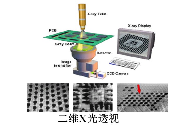
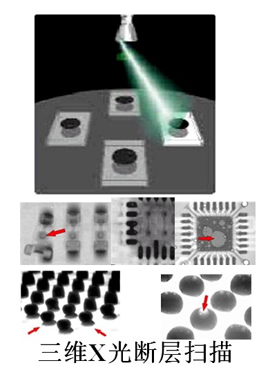
X optical detection
The resolution suitable for board-level circuits is about 5-20 microns.
The application of X-ray inspection technology in board-level circuit assembly only began to be applied to board-level circuit manufacturing of military electronic equipment in the early 1990s. New packaging devices such as PGA, BGA, and CSP on the PCBA of electronic products are widely used.
There may be risks in the detection of certain components (such as crystal oscillators) by X-rays.


4. Component installation
1) Insertion:
Forming: whether the lead length, shape, span, and marking meet the product and process requirements;
Plug-ins: the distribution of wrong parts, missing parts, reverse, component damage, kneeling, missing parts;
The reasonableness of the process.
2) Surface mount parts:
Statistics of wrong parts, missing parts, missing parts, reverse parts, reverse parts and offsets;
Lost item rate; accuracy rate.
5. Inspection and testing
1) Detection:
Misjudgment rate: detection standard database, test strategy;
Detection rate: Failed to detect content distribution.
2) Inspection:
Missing rate;
Qualification level of personnel.
manual visual inspection
flexible;
limited to superficial inspection;
low efficiency;
poor consistency
High labor intensity, easy to fatigue;
Fault coverage is only about 35%;
High-density, fine-pitch PCB inspection is mainly carried out with the help of a magnifying glass of about 5-40 times
 Meizhou Ruiputuo Technology Co.,Ltd