After drawing the schematic library of the components, it is necessary to design the PCB package library of the components with more stringent conditions, otherwise it will not be possible to design the subsequent PCB layout.
The PCB package drawing is generally carried out together with the schematic diagram design, that is, the PCB package drawing of the components is carried out at the same time after the schematic diagram parameters of the components are drawn.
The packaging of the PCB is actually the size of the electronic components, the size of the pad, the length and width of the pins (these parameters can be found in the specifications of the components) in the form of graphics, and the requirements for these parameters are also very strict. Strictly, the size cannot be deviated or only a certain range of deviation is allowed.
After knowing the specific physical parameters of the components, the production of the PCB package can be officially started. Open the pads Layout software for the corresponding PCB design.
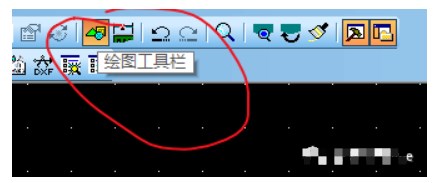
Select the option to create a new library component, and then click the "Drawing Toolbar" to make all the drawings.
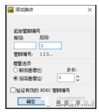
First of all, for the placement of pads, click Add Endpoint to set. The default is to start with 1, and the number of endpoint pads added later will increase in turn.
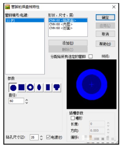
The characteristics of the pad can also be changed, such as the shape, size, size, etc. of the pad, as shown in the figure below.
After the first pad is made, if the following pads are regular (for example, multiple pins have the same pitch), you can use "distribution and repetition" like making schematic diagrams
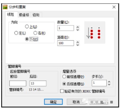
It can be seen that it supports the distribution and repetition of the four directions of up, down, left, and right, which can greatly improve the convenience and accuracy of production during the production process.
It is worth mentioning that PADS supports the distribution and repetition between different directions, that is to say, a horizontal pad can get a vertical pad by setting the direction up or down, just need to design and calculate the distance , so it will be very convenient when drawing some IC pin pads.
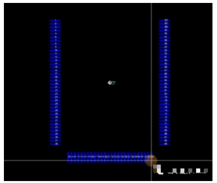
For the length of the pin, generally add a distance of 0.4 to 0.5 mm (also called compensation) based on the length of the original device. Generally, compensation is not performed for the width, because compensation may lead to tin connection.
After the pins are drawn, it is time to draw the internal border. Directly select the 2D line in the drawing toolbar, select a rectangle to draw, and if there are too many pins, you need to draw a pin mark, usually a circle.
After all the drawing is completed, it can be saved to get the final PCB package.
But how to associate with the schematic diagram after the PCB package design is completed?
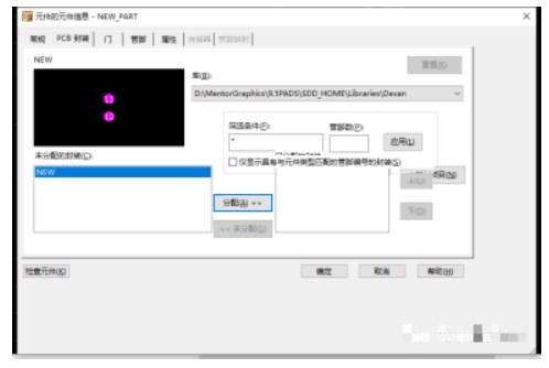
This operation needs to be performed in the PADS Logic software. After selecting the corresponding components, and then click Assign, you can bind the PCB package with the corresponding schematic diagram
。
Finally, there is another point that needs special attention, that is, for the setting of the origin, the coordinates of the origin are (0, 0), so after setting the origin, judge the size of the entire PCB package according to the distance from the origin, and determine the relative position , otherwise it will lead to deviations in the size of the components.
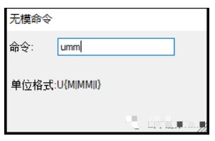
Other notes: Change the display unit of the size, such as the conversion between mm (millimeter) and mil (directly input umm)
。
 Meizhou Ruiputuo Technology Co.,Ltd