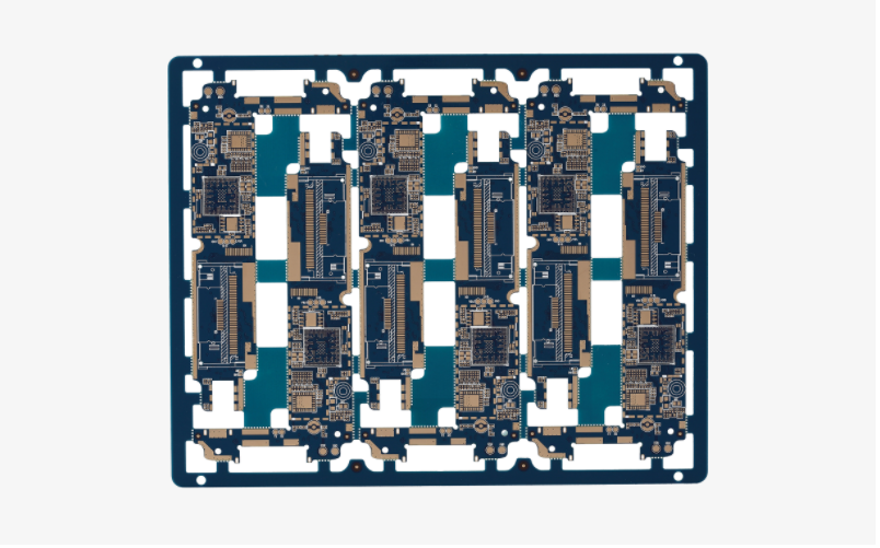
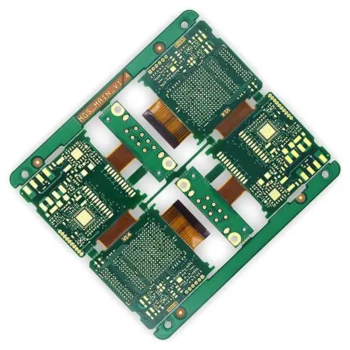
This structure of HDI PCB contains 1 “build-up” of high-density interconnection layers, suitable for BGA with lower I/O counts.
It has fine lines, microvia and registration technologies capable of 0.4 mm ball pitch, excellent mounting stability and reliability, and may contain copper filled via.
Applications: Cell phone, MP3 Player, GPS, Memory Card.
HDI PCB (1+N+1)

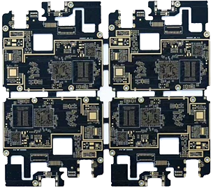
HDI PCB (2+N+2): Moderate Complex HDI
This structure of HDI PCB contains 2 or more “build-up” of high-density interconnection layers; microvias on different layers can be staggered or stacked; Copper filled stacked microvia structures are commonly seen in challenging designs that demand high level signal transmission performance.
These are suitable for BGA with smaller ball pitch and higher I/O counts and can be used to increase routing density in a complicated design while maintaining a thin finished board thickness.
Applications: Cell phone, PDA, game console, portable video recording devices.
HDI PCB (2+N+2)

ELIC (Every Layer Interconnection): Most Complex HDI
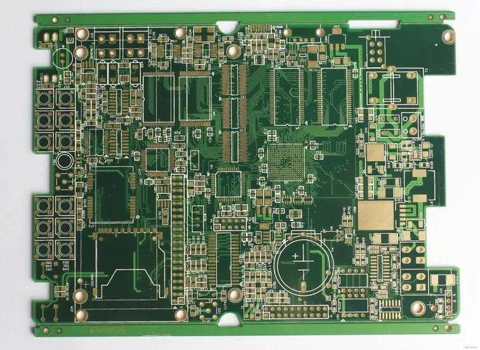
In this HDI PCB structure, all the layers are high-density interconnection layers which allow the conductors on any layer of the PCB to be interconnected freely with copper filled stacked microvia structures.
This provides a reliable interconnect solution for highly complex large pin-count devices, such as CPU and GPU chips utilized on handheld and mobile devices while producing superior electrical characteristics.
Applications: Cell phone, ultra-mobile PC, MP3, GPS, Memory cards, small computer devices.
ELIC (Every Layer Interconnection)

PCB International strongly recommends sending us the Board Stackup to sales@rpttechpcb.com so we may confirm your desired HDI board design can be successfully manufactured.
rpttechpcb is Professional production low-cost PCB,Cheap PCB, Low price for PCB,94V0
 Meizhou Ruiputuo Technology Co.,Ltd