Meizhou Ruiputuo Technology Co.,Ltd
 What is the key to designing real circuit boards on paper or any physical form? Let's explore the first 5 design guidelines that can be understood when designable and reliable PCB.
5 major PCB design guidelines for engineers
At the beginning of new design, because most of the time spent on circuit design and component selection, it is often not thorough enough due to lack of experience in the PCB layout wiring stage. If you do not provide sufficient time and energy for the design of the PCB layout stage, it may cause the design to transform from the digital field to physical reality, problems occur during the manufacturing stage, or have defects in terms of function. So what is the key to design a true and reliable circuit board on paper and physical forms? Let's explore the first 5 PCB design guidelines that can be understood by designing a manufacture and reliable PCB.
No. 1 -Filter your component layout
The component placement stage of the PCB layout process is both science and art, and it is necessary to strategically consider the main components available on the circuit board. Although this process may be challenging, you will determine the difficulty of making your circuit board and how it meets your original design requirements.
Although the conventional universal order of components is placed in order, such as the installation device, power circuit, precision circuit, key circuit, etc. of the connecter, printing circuit board, etc., there are also some specific guidelines that need to be kept in mind, including: including:
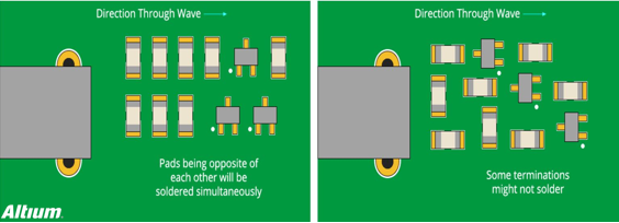
Diversion -to ensure that similar components are positioned in the same direction, which will help achieve efficient and error -free welding processes.
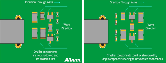
Arranging -Avoid placing smaller components behind larger components, so that small components may be affected by large components welded and cause installation and paste.
Organization -It is recommended to place all surface installation (SMT) components on the same side of the circuit board, and place all the pores (TH) components on the top of the circuit board to minimize the assembly steps.
Finally, pay attention to a PCB design guide -that is, when using hybrid technology components (through holes and surface stickers), manufacturers may need additional processes to assemble circuit boards, which will increase your overall cost
。
良好的芯片元件方向(左)和不良的芯片元件方向(右)
良好的元件布置(左)和不良元件布置(右)
No. 2 -Appropriate Power Placement, grounding and signal wiring
After the components are placed, the power, grounding and signal wiring can be placed next to ensure that your signal has a clean path of clean and non -failure. At this stage of the layout, please remember the following criteria:
Positioning power supply and grounding plane layer
It is always recommended to place the power and ground plane layer inside the circuit board, while maintaining symmetry and centering. This helps to prevent your circuit board bent, which is also related to whether your components are correctly located. For power supply to IC, it is recommended to use a public channel for each power supply to ensure a strong and stable width width of the line, and avoid the chrysanthemum chain power connection between components and components.
Signal line connection
Next, connect the signal line according to the design situation in the schematic diagram. It is recommended to always take as short paths and direct paths between components. If your component needs to be placed in the horizontal direction without deviation, it is recommended to go on the horizontal line in the place where the component of the circuit board is out, and then the vertical wiring is performed after the line. In this way, with the migration of the weld, the element will be fixed in the horizontal direction. As shown in the first half of the figure below. The signaling method in the lower half of the figure below. As the solder flows during welding, it may cause the component's partial rotation
建议的布线方式 (箭头指示焊料流动方向)
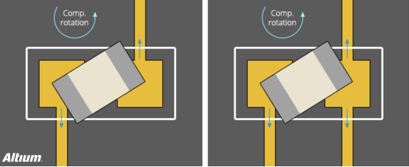
不建议的布线方式 (箭头指示焊料流动方向)
Define network width
Your design may require different networks. These networks will carry various currents, which will determine the width of the network required. Considering this basic requirements, it is recommended to provide 0.010 '(10mil) width for low -current analog and digital signals. When your circuit current exceeds 0.3 amp, it should be widening. Here is a free line width calculator to make this conversion process simple.
No. 3 -Effective isolation
You may have experienced how large voltage and current peaks in the power circuit interfere with your low -voltage current control circuit. To minimize the problem of such interference, follow the following guidelines:
Isolation -Make sure that each power supply keeps the power space and control the ground. If you have to connect them together in PCB, make sure it as close to the end of the power path as much as possible.
Arranging -If you have placed a horizon on the middle layer, make sure to place a small impedance path to reduce the risk of any power circuit interference and help protect your control signal. You can follow the same guidelines to keep your numbers and simulation separation.
Coupling -In order to reduce the capacitor coupling of the large horizon and the capacitor coupling above and below, try only to cross the simulation floor through analog signal line.No. 4 -Solution of calories
Have you ever caused a reduction in circuit performance due to calorie problems or even damage to the circuit board? Because there are no considering heat dissipation, many problems have plagued many designers. Here are some guidance to remember to help solve the problem of heat dissipation:
Identification of troublemaking components
The first step is to start considering which components will dissipate the maximum calories on the circuit board. This can be achieved by finding the "thermal resistance" level in the data table of the component, and then the heat generated by the guidance policy of the suggestion is based on the proposed guidelines. Of course, the heat sink and cooling fan can be added to keep the component temperature decrease, and remember to keep the key components away from any high heat source.
Add heating wind pad
Add heating wind pads is very useful for production can be manufactured. They are essential for high copper content components and multi -layer circuit boards. Because it is difficult to maintain the process temperature, it is always recommended to use the hot air pads on Tongkou elements to make the welding process as simple as possible by slowing the heat dissipation rate at the foot of the component.
As a general guideline, it is always connected to any pore or over -perforated hot air pads connected to the ground plane or power plane. In addition to the hot wind pad, you can also add tears to the position of the pad connection line to provide additional copper foil/metal support. This will help reduce mechanical stress and thermal stress.
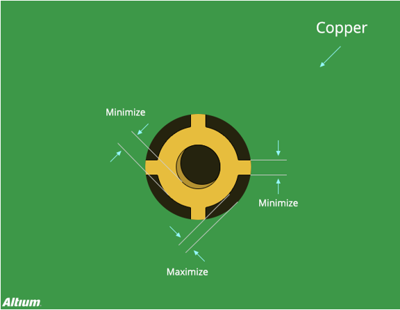
典型的热风焊盘连接方式
Science popularization of hot wind pad:
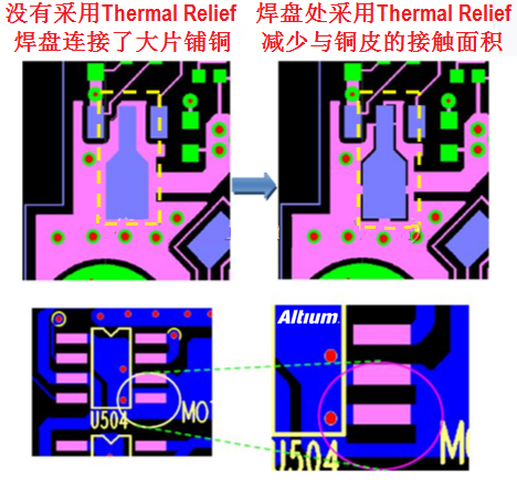
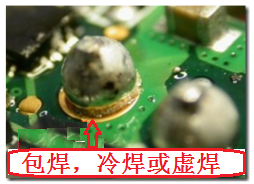
Many factories are responsible for the process (Process) or SMT technology. NON-Wetting's adverse problems, no matter how the process conditions are changed or how to adjust the furnace temperature of the stream welding, there is a certain ratio that cannot be welded. what on earth is it?
Leaving aside the oxidation of components and circuit boards, after the root cause, it is found that a large part of this type of welding is actually from the laboratory design of the circuit board, and the most common thing is that some of the welding in the component is some of the welding of the component. The feet are connected to a large area of copper leather, causing these components to welded the feet after returning and welded in poor welding. The components are welded.
Generally, PCB often needs to laid large -area copper foil in circuit design to be used as a power supply (VCC, VDD or VSS) and ground (GND, GROUND). These large -area copper foils are generally connected directly to some control circuits (ICs) and electronic components.
Unfortunately, if we want to heat these large -area copper foil to the temperature of tinning, it usually takes more time than the independent welding pads (that is, the heating will be slower), and the heat dissipation is relatively fast. When such a large area of copper foil wiring is connected to small components such as small resistors and small capacitors, and the other end is not, it is easy to cause welding problems due to inconsistent tin merging and solidification time; Instead of adjusting, when the warm -up time is insufficient, these components connected to large copper foil feet are easy to cause virtual welding due to the failure of the tinning temperature.
When manual welding, these component welding feet connected to large copper foil will not be welded within the specified time because the heat dissipation is too fast. The most common adverse phenomenon is welding and virtual welding. The solder is only soldering on the welding foot of the component without connecting to the circuit board pad. From the appearance, the entire welding joint will form a spherical shape; even more, the operator continues to increase the temperature of the soldering iron to welded the welding foot on the circuit board, or heated too long, causing the component to exceed the thermal resistance temperature and the temperature resistance temperature and the heat resistance temperature and Destroy and not know. As shown below.
Now that we know the problem, there can be solutions. Generally, we will require the so -called Thermal RELIEF PAD. As shown in the figure below, the wiring on the left does not use hot air pads, and the wiring on the right has adopted the connection method of hot air pads. You can see that the contact area of the pad and large copper foil is only a few small lines. This can greatly limit the loss of temperature on the welding pad to achieve a better welding effect.