 Meizhou Ruiputuo Technology Co.,Ltd
 As we all know, impedance control is the most basic principle of our high-speed design. At present, conventional board factories will control the impedance within 10% error, and many friends will have doubts, why is it 10%? Theoretically, the smaller the error, the better, so why can't the conventional control ability be further pushed to 8%, or even 5%?
The ideal is beautiful, but the reality is inevitably "cruel". There are many factors that affect the impedance of PCB traces, mainly including the width of the copper wire, the thickness of the copper wire, the dielectric constant of the medium, the thickness of the medium, and the thickness of the solder mask. Therefore, if you want to make the impedance error small, you need to control the errors of the above factors very well during the PCB processing process, so that the final impedance error will be small.
But from the PCB processing technology step by step, you will find that almost every process will produce errors in the transmission line impedance control, and some processes are full of randomness, so the value of 10% is obtained after the board factory integrates various errors. A relatively optimal value that can be achieved has come out. And 8% or even 5% is very difficult to achieve.
Difficulty 1: Glass fiber effect
It can be seen from the PCB slice that the PCB medium (whether it is core or PP sheet) is composed of two parts, including glass fiber cloth (glass fiber cloth) and resin. Among them, the glass fiber cloth is like a skeleton, which plays the role of increasing strength and support, and the resin is like glue, which plays the role of bonding.
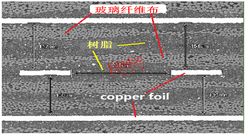
What is the glass fiber effect? The glass fiber effect is caused by the different dielectric constants of glass fiber cloth and resin. Generally speaking, the dielectric constant of glass fiber cloth is about 6, while that of resin is relatively low, generally between 2-3. At this time, where the differential line is located on the glass fiber cloth is very important: when it falls on the empty window and on the cloth, the corresponding impedance difference is relatively large, which will cause impedance errors.
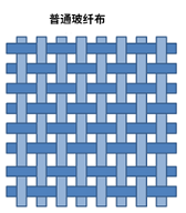
The structure of ordinary glass fiber cloth: there are empty windows
The influence of the glass fiber effect on the impedance is mainly because the trace may fall on the empty window or on the glass fiber cloth. Due to the difference in the dielectric constant between the two, the impedance shown must be different.
In actual production, it is full of randomness whether the wiring will fall on the empty window or on the glass fiber cloth, so the impedance error caused here is uncontrollable.
Difficulty 2: Line width/line thickness precision error control
Line width is one of the important factors affecting impedance: the larger the line width, the lower the impedance. In the PCB production process, the line width needs to be controlled within a tolerance of 10% in order to better meet the impedance control requirements. Similarly, line thickness (copper thickness) is also one of the important factors affecting impedance: the thicker the copper, the smaller the impedance.
But in actual production, poor line precision control and large impedance deviation are the most common problems for many PCB manufacturers. To control the accuracy of the circuit, PCB manufacturers must have high-quality circuit exposure machines and vacuum etching machines. In order to ensure that the line width is as consistent as possible, the board factory also needs to perform process compensation on the engineering film according to the amount of etching side erosion, photo-drawing error, and graphic transfer error, so as to meet the line width/thickness requirements.
Difficulty 3: Media thickness control
Increasing the dielectric thickness can increase the impedance, and reducing the dielectric thickness can reduce the impedance.
Different curing sheets have different glue content and thickness, so the board factory needs to accurately understand the medium thickness of the board itself; at the same time, the thickness of the board after lamination is related to the flatness of the press and the program of the pressing board. Therefore, if the plate factory wants to control the thickness of the medium, the key lies in engineering design, platen control, and incoming material tolerance. Any problem in the process will affect the final impedance error of the board.
Especially for high multi-layer impedance boards, the lamination process is very critical. Because the PP dielectric layer will show a state of glue flow under high temperature lamination, at this time, the temperature, process, and calibration control of the lamination are very critical, otherwise the thickness deviation of the finished dielectric layer will seriously affect the accuracy of the impedance value.
Difficulty 4: Solder mask thickness control
In general, printing the solder mask will reduce the impedance of the outer layer, so the influence of the solder mask will be taken into account when controlling the impedance error. Under normal circumstances, printing the solder mask once can make the single-end drop 2Ω, and the differential drop can be 8Ω; the drop value of printing twice is twice that of one pass; when printing more than three times, the impedance value will not change.