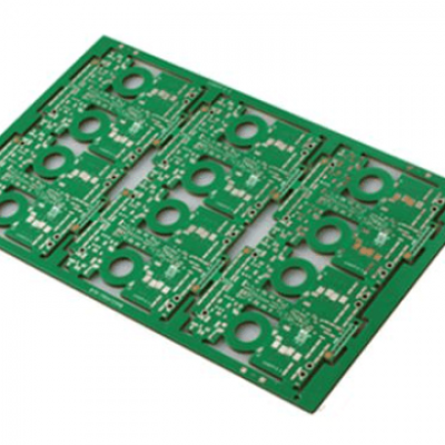
Due to their small size and size, there are few ready-made printed circuit board standards for the growing wearable IoT market. Before these standards came out, we had to rely on what we learned in board-level development and manufacturing experience, and think about how to apply them to unique emerging challenges. There are three areas that require our particular attention: board surface materials, RF/microwave design, and RF transmission lines.
PCB material
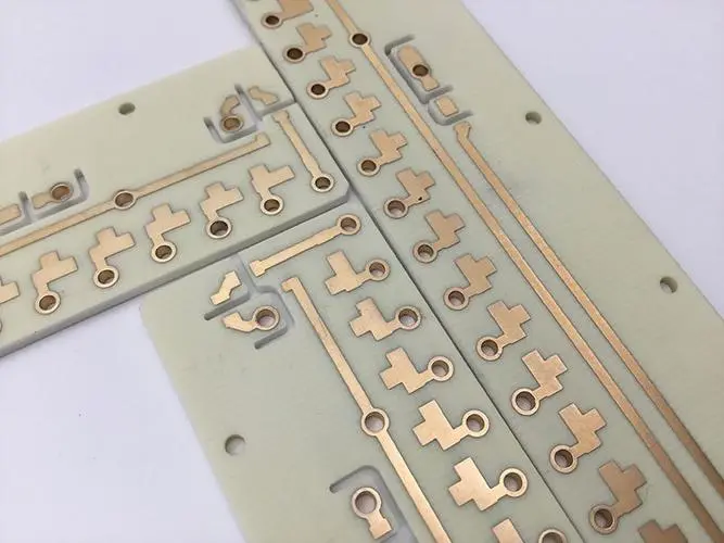
PCBs generally consist of laminates that may be fabricated from fiber-reinforced epoxy (FR4), polyimide, or Rogers material, or other laminated materials. The insulating material between the different layers is called a prepreg.
Wearable devices require high reliability, so this becomes an issue when PCB designers are faced with the choice of using FR4 (the most cost-effective PCB manufacturing material) or more advanced and more expensive materials.
If a wearable PCB application requires high-speed, high-frequency materials, FR4 may not be the best choice. FR4 has a dielectric constant (Dk) of 4.5, the more advanced Rogers 4003 series materials have a dielectric constant of 3.55, and sibling series Rogers 4350 has a dielectric constant of 3.66.
the

The dielectric constant of a stack is the ratio of the capacitance or energy between a pair of conductors in the vicinity of the stack to the capacitance or energy between the pair of conductors in vacuum. At high frequencies, it is desirable to have very little loss, so Roger 4350, which has a dielectric constant of 3.66, is more suitable for higher frequency applications than FR4, which has a dielectric constant of 4.5.
Normally, the number of PCB layers used in wearable devices ranges from 4 to 8 layers. The principle of layer construction is that if it is an 8-layer PCB, it should provide enough ground and power layers and sandwich the wiring layer in the middle. In this way, ripple effects in crosstalk are kept to a minimum and electromagnetic interference (EMI) is significantly reduced.
In the stage of circuit board layout design, the layout scheme is generally to place a large ground layer close to the power distribution layer. This can form a very low ripple effect, and the system noise can be reduced to almost zero. This is especially important for radio frequency subsystems.
Compared with Rogers material, FR4 has a higher dissipation factor (Df), especially at high frequencies. For higher performance FR4 stacks, the Df value is around 0.002, which is an order of magnitude better than normal FR4. But Rogers stacks are only 0.001 or less. When FR4 material is used for high frequency applications, there will be a noticeable difference in insertion loss. Insertion loss is defined as the power loss of a signal traveling from point A to point B when using FR4, Rogers or other materials.
create problems
Wearable PCBs require tighter impedance control, which is an important factor for wearable devices, and impedance matching can result in cleaner signal transmission. Earlier, the standard tolerance for signal-carrying traces was ±10%. This indicator is obviously not good enough for today's high-frequency and high-speed circuits. The current requirement is ±7%, and in some cases even ±5% or less. This parameter, along with other variables, can severely impact the manufacture of these wearable PCBs with particularly tightly controlled impedance, limiting the number of vendors that can manufacture them.
The dielectric constant tolerance of laminates made of Rogers UHF materials is generally maintained at ±2%, and some products can even reach ±1%. In contrast, the dielectric constant tolerance of FR4 laminates is as high as 10%. Therefore, comparison Rogers' insertion loss can be found to be particularly low for these two materials. Compared with traditional FR4 material, the transmission loss and insertion loss of the Rogers laminate are half that.
Cost matters most in most cases. However, Rogers offers relatively low loss high frequency stack performance at an acceptable price point. For commercial applications, Rogers can be used with epoxy-based FR4 to make a hybrid PCB, where some layers use Rogers material and other layers use FR4.
Frequency is the primary consideration when selecting a Rogers stackup. When the frequency exceeds 500MHz, PCB designers tend to choose Rogers materials, especially for RF/microwave circuits, because these materials can provide higher performance when the traces above are strictly controlled by impedance.
Compared with FR4 material, Rogers material also offers lower dielectric loss, and its dielectric constant is stable over a wide frequency range. In addition, Rogers materials can provide the ideal low insertion loss performance required for high frequency operation.
The coefficient of thermal expansion (CTE) of Rogers 4000 series materials provides excellent dimensional stability. This means that when the PCB goes through cold, hot and very hot reflow cycles, the thermal expansion and contraction of the board can be maintained at a stable limit at higher frequency and higher temperature cycles compared to FR4.
In a hybrid stackup scenario, it is relatively easy to achieve high manufacturing yields by mixing Rogers and high-performance FR4 using common manufacturing process technologies. Rogers stackup does not require a dedicated via preparation process.
Ordinary FR4 cannot achieve very reliable electrical performance, but high-performance FR4 materials do have good reliability characteristics, such as higher Tg, are still relatively low cost, and can be used in a wide variety of applications, from simple audio design to complex microwave applications.
the
RF/Microwave Design Considerations
Portable technology and Bluetooth pave the way for RF/microwave applications in wearable devices. Today's frequency ranges are becoming more and more dynamic. A few years ago, very high frequency (VHF) was defined as 2GHz~3GHz. But now we can see ultra-high frequency (UHF) applications ranging from 10GHz to 25GHz.
theTherefore, for wearable PCBs, the radio frequency part requires closer attention to wiring issues, and the signals should be separated separately to keep the traces that generate high-frequency signals away from the ground. Other considerations include: providing bypass filters, adequate decoupling capacitors, grounding, and designing transmission and return lines to be nearly equal.
theBypass filters suppress noise content and ripple effects of crosstalk. Decoupling capacitors need to be placed closer to the device pins that carry power signals.
theHigh-speed transmission lines and signal loops require a ground plane between power plane signals to smooth out jitter from noisy signals. At higher signal speeds, small impedance mismatches can cause unbalanced transmit and receive signals, resulting in distortion. Therefore, special attention must be paid to impedance matching issues related to radio frequency signals, because of the high speed and special tolerance of radio frequency signals.
theRF transmission lines require controlled impedance in order to carry RF signals from a specific IC substrate to the PCB. These transmission lines can be implemented in the outer, top and bottom layers, or can be designed in the middle layer.
theMethods used during PCB RF design layout are microstrip, suspended stripline, coplanar waveguide or grounding. A microstrip line consists of a fixed length of metal or trace with all or part of a ground plane directly below it. The characteristic impedance in the general microstrip line structure is from 50Ω to 75Ω.
the

Floating striplines are another method for routing and suppressing noise. This line consists of fixed-width traces on inner layers and a large ground plane above and below the center conductor. The ground plane is sandwiched between the power planes and thus provides a very effective grounding effect. This is the preferred method for routing RF signals on wearable PCBs.
theCoplanar waveguides can provide better isolation near RF lines and lines that need to be traced close together. This medium consists of a center conductor surrounded by ground planes on either side or below. The best way to route RF signals is with suspended striplines or coplanar waveguides. These two methods provide better isolation between signal and RF traces.
theIt is recommended to use so-called "via fences" on both sides of the coplanar waveguide. This approach provides a row of ground vias on each metal ground plane in the center conductor. The main trace running in the middle has fences on each side, thus giving the return current a shortcut to the formation below. This approach reduces the noise level associated with high ripple effects on RF signals. The dielectric constant of 4.5 remains the same as the prepreg FR4 material, while prepregs—from microstrip, stripline, or offset stripline—have a dielectric constant of about 3.8 to 3.9.

In some devices that use a ground plane, blind vias may be used to improve decoupling from the power supply capacitors and provide a shunt path from the device to ground. A shunt path to ground shortens the via length, which serves two purposes: not only do you create a shunt or ground, but you reduce the reach for devices with small grounds, which is an important RF design factor.
 Meizhou Ruiputuo Technology Co.,Ltd