The number of PCB board resolution layers is as follows:
1. Single-sided PCB
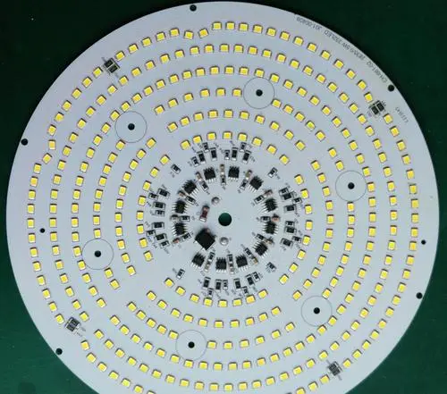
That is, only one side of the PCB board has lines (with or without holes), and the other side is covered with substrate or direct insulating ink, without any lines, and the whole board is light-transmitting under strong light (except for individual boards and special processes. Requirements), the cross-section only contains copper foil on the side with lines;
2. Double-sided PCB
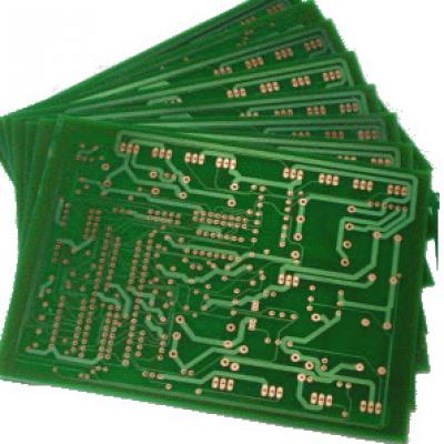
It is generally common that there are lines on both sides, relying on copper holes as the "bridge" connecting the two sides of the board and placing the entire PCB board under strong light to transmit light (except for individual boards and special process requirements), the cross-section is only the outermost two sides of the PCB board Contains copper foil;
3. Multi-layer PCB
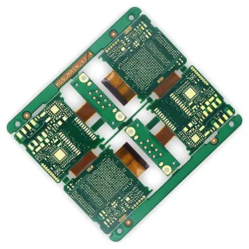
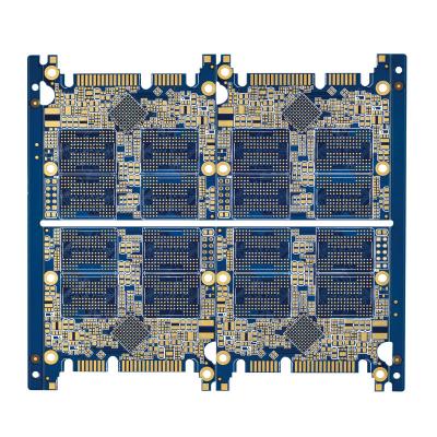
On the basis of the double panel, there is a sandwich PCB in the middle like a "sandwich" (see manufacturing capabilities, general mobile phones, computers, home appliances, 4 to 12 layers of automobiles; military or aviation, positioning, 8 to 20 layers; satellite, navigation , rockets, etc. can reach more than 60 layers, and its precision can be imagined. In fact, the CPU can also be understood as an ultra-precision "PCB" in microelectronics) The interlayer in the middle is generally called the "inner layer".
The multi-layer PCB is opaque or partly transparent under strong light and is not obvious. The outermost ends and the middle of the cross-section contain copper foil.
In the case of single-sided, double-sided, and multi-layer PCBs with the same board and the same volume, the weight of multi-layer PCB > the weight of double-sided PCB > the weight of single-sided PCB


 Meizhou Ruiputuo Technology Co.,Ltd


