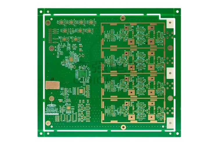
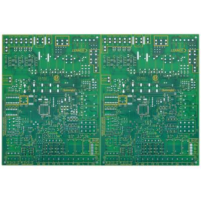
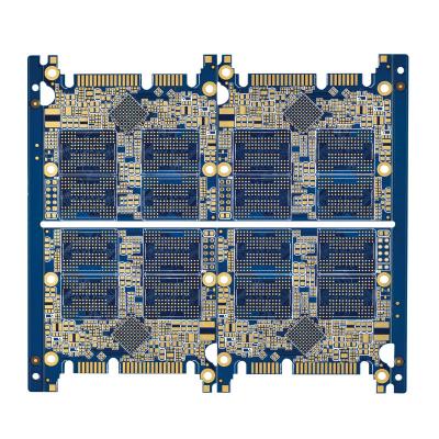
Under the opportunity of large-scale commercial use of 5G next year, mobile phone motherboards will usher in deterministic major changes due to chip upgrades, and relevant manufacturers will benefit significantly: 1) The penetration rate of Anylayer motherboards in the Android system will increase, and the tight supply will make mainland manufacturers have Entry opportunities; 2) Apple's SLP is fully upgraded, and the unit price is expected to increase significantly. In addition, the supply structure is stable, and core companies will benefit significantly.
1. HDI is a high-density solution, and 5G drives supply and demand reversal
1.1. The high density of HDI determines that its main application lies in mobile phones
The HDI board is a High Density Interconnect multilayer board (High Density Interconnect), which is a subdivided board type in rigid circuit boards. The compound growth rate reaches 5.9%, which is second only to the flexible board (FPC)

What are HDIs? HDI is actually a concept relative to ordinary through-hole multilayer boards. Its characteristic is that there are many micro-blind holes/buried blind holes inside. It can be said that a PCB board drilled with micro-blind holes/buried blind holes is HDI. Looking further, micro-blind vias/buried blind vias are generally realized by adding layers, and HDI can be divided into first-order HDI, second-order HDI, third-order HDI, and arbitrary layer HDI 1 ( Anylayer HDI is the highest-level HDI, hereinafter referred to as Anylayer).

The main characteristic of HDI is high density. Due to the existence of many micro blind holes/buried blind holes in HDI, its wiring density is higher than that of through-hole boards. The principle is:
1) Blind/buried blind holes can save wiring space. Ordinary multi-layer boards use through holes to connect different layers, but through holes will take up a lot of space that could be used for wiring. On the contrary, using blind holes/buried blind holes to realize the connection function between different layers can free up space for more Wiring, thereby increasing the density of wiring;
2) Laser drilling can reduce the aperture. Blind holes/buried blind holes mostly use laser drilling to burn off the resin dielectric layer, and through holes are usually made by mechanical drilling (laser lasers are difficult to penetrate the copper surface or are very time-consuming), compared with the diameter of laser drilling It is thinner than mechanical drilling (if the diameter of mechanical drilling is to reach the same size as laser drilling, a very thin drill bit is required, and the thin drill bit is easy to break and the cost is high), saving space.
Therefore, the more blind vias/buried blind vias are used, the higher the density, that is to say, the higher the order of HDI, the higher the density. Anylayer is the board type with the highest density in HDI. However, it is worth noting that after HDI is upgraded to Anylayer, it is no longer possible to increase the wiring density by increasing blind holes/buried blind holes. It can be seen that HDI is an important board to achieve high-density wiring.


1.2. Why pay attention to HDI now? The main logic is that 5G will change the supply and demand pattern
According to the above, it can be known that the development trend of HDI mainly depends on mobile phones, and changes in mobile phones will have a profound impact on HDI. From the current point of view, the biggest change point of mobile phones is the evolution from non-5G to 5G. The underlying logic of this change is that the chip size of 5G mobile phones will be smaller and the integration level will be improved. As the main carrier of chips, mobile phone motherboards will inevitably be upgraded. We believe that the upgrade logic and supply and demand logic of Android-based and Apple-based mobile phone motherboards are different. Specifically:
1) Android system: The supply gap is 20%, and the domestic industry chain welcomes entry opportunities.
Demand side: 1/2 level → Anylayer. HDI is mainly used on the motherboard of Android mobile phones. The low-end and middle-end phones mainly use first-order/second-order HDI, and only high-end machines use third-order and above HDI. However, 5G mobile phones have higher requirements for line width, line spacing, and aperture. Therefore, next year 5G Mobile phones must adopt Tier 4 or above HDI (anylayer technology is basically used for Tier 4 and above), and 5G mobile phones are expected to sink to mid- and low-priced models next year. It can be seen that Android's demand for high-end HDI (Anylayer) has doubled.
Supply: Double consumption of production capacity + insufficient reserves for expansion + strict environmental impact assessment. As the number of stages increases, the production capacity is doubled. The production capacity of the second stage of the same lamination production line is only 50% of that of the first stage; after Apple gave up the Anylayer solution, the high-end Anylayer production capacity was idle, so the supply-side expansion attitude Not active, and the expansion of Anylayer is limited by the environmental impact assessment review, making it difficult to expand production capacity in a timely manner.
How to look at next year: production capacity is short of 20%, and domestic suppliers welcome opportunities. According to our calculations, the Anyalyer supply and demand gap will reach 20% of the original production capacity in 2020. In this case, on the one hand, suppliers will increase prices, and on the other hand, mobile phone terminal manufacturers will introduce new suppliers, domestic manufacturers with Anylayer technology There will be an opportunity to enter.
2) Apple series: The unit price of motherboards has risen, and existing players have become beneficiaries.
Requirements: Increase the value of SLP stand-alone machines. There are two main changes in Apple motherboards. On the one hand, Apple’s old models that do not use SLP will be upgraded from Anylayer to SLP. On the other hand, the SLP motherboards of new 5G models will be further upgraded (ASP increased by 30%), and the average value of a single machine will increase. .
Supply: Capacity matches demand. There are still few Android-based models that use SLP motherboards. The global SLP production capacity mainly serves Apple, and the production capacity layout arrangement is well grasped, so the supply is guaranteed.
How to see next year: the profitability of existing players will increase. Since SLP has a higher technical threshold than ordinary HDI, and Apple's certification threshold is also higher, it is difficult for HDI manufacturers to get involved in this category in the short term. Boom, changing production to SLP does not have economic benefits, so the SLP structure will be relatively stable next year, and existing players can enjoy the bonus of product upgrades.
To sum up, under the opportunity of large-scale commercial use of 5G next year, mobile phone motherboards will usher in deterministic major changes due to chip upgrades, and relevant manufacturers will benefit significantly. We are optimistic about Pengding Holdings (with both SLP and Anylayer HDI capabilities) and Dongshan Precision. We recommend paying attention to: Founder Technology, Ultrasonic Electronics, and Zhongjing Electronics. Below we will explain in detail from the two aspects of Android and Apple.
2. The 5G chip forces the motherboard to be upgraded, and the Android and Apple systems are fully upgraded
2.1. The 5G chip is highly integrated and small in size, and the 5G motherboard will fully adopt Anylayer and SLP
From the current point of view, the biggest change related to mobile phones is the transformation from non-5G mobile phones to 5G mobile phones, and the underlying change logic is the change of chips. Chip changes mainly come from two aspects:
1) 5G increases the number of RF front-end chips: the number of RF front-end chips in the mobile phone will increase correspondingly with the increase of the communication frequency band (generally, one chip handles one frequency band). Since the 5G mobile phone increases the 5G communication frequency band, the number of chips in the 5G mobile phone will increase. Increase;
2) The number of I/Os of 5G chips will increase: With the increasingly complex functions and faster response speed of mobile phones, 5G mobile phones will have stronger capabilities in terms of computing power and storage capacity, which will eventually be reflected in More I/O counts. If the chip process remains the same, more I/O counts mean larger chip size.
The above two major changes mean that if the mobile phone chip technology does not change substantially, the number and size of the chips will be larger, which will require more motherboard space. The motherboards of Huawei Mate 20 X 5G and Mate 20 Pro (4G) For example, using the same 12-layer Anylayer technical solution, the motherboard area of Mate 20 X 5G is 17~20cm2 larger than that of Mate 20 Pro.

Therefore, in the case of the limited size of the mobile phone itself, it is imperative to increase the integration level of the chip (reduce the number) and adopt a lower nanometer process (control the size). According to the 5G chips released by major chip manufacturers, we can see that the main 5G chips that have been released will basically adopt the process technology within 7nm (only Samsung Exynos980 adopts the 8nm process, but this is not the main model and has little impact ), and Qualcomm’s Snapdragon 765G and HiSilicon’s Kirin 990 “integrated version” both integrate SoC and 5G baseband, which shows that the trend of 5G chips with high integration and low nanometer process is determined.
The solution of high chip integration and low nanometer process is simply to make more circuits (high integration) in a smaller area (low nanometer process), which will inevitably reduce the BGA diameter and pad pitch , Correspondingly, the line width and line spacing, aperture size, etc. of the mobile phone motherboard that carries the chip must also be reduced.
According to the foregoing, the high density of HDI is achieved by adding blind holes/buried blind holes by adding layers. The smaller it is, that is to say, the adoption of high-end solutions is the only way to reduce the line width and spacing/aperture size of the main board. According to academic literature, the minimum theoretical line width and line spacing of HDI, Anylayer, and SLP can reach 50um, 35um, and 25um. With reference to the motherboard solutions and corresponding characteristic parameters of Apple’s various models, it can be inferred that the 5G mobile phone chips are highly integrated and small. In the case of size, the trend of upgrading mobile phone motherboards from HDI to Anylayer and then to SLP is accelerating.
According to industry chain research, next year 5G mobile phones will adopt at least fourth-order HDI process technology, that is, shift to Anylayer and SLP solutions. Specifically, the changes between the Android system and the Apple system are different:
1) Two changes in the Android system: the mainboard of the model that originally used the Anylayer motherboard continues to be upgraded + the model that did not use the Anylayer motherboard uses Anylayer;
2) Two changes in the Apple system: the original model with Anylayer motherboard is upgraded to SLP + the original model with SLP motherboard continues to be upgraded

 Meizhou Ruiputuo Technology Co.,Ltd


