Commonly Used Terms In PCB Assembly
What the Heck Is Your PCB Vendor Talking About? – Common Terms for PCB Assembly
 Every industry has its established lingo, which helps its members communicate more efficiently. If you are on the outside looking in, however, it can seem like they are speaking a foreign tongue. This becomes a problem when you need to work with vendors on ordering printed circuit boards for your device or your prototype. If you’ve gotten lost while trying to speak to your vendor (SMP, SME, SMD?), then you’ve come to the right place. Here is our no-nonsense guide on the most common terms in the printed circuit board industry:
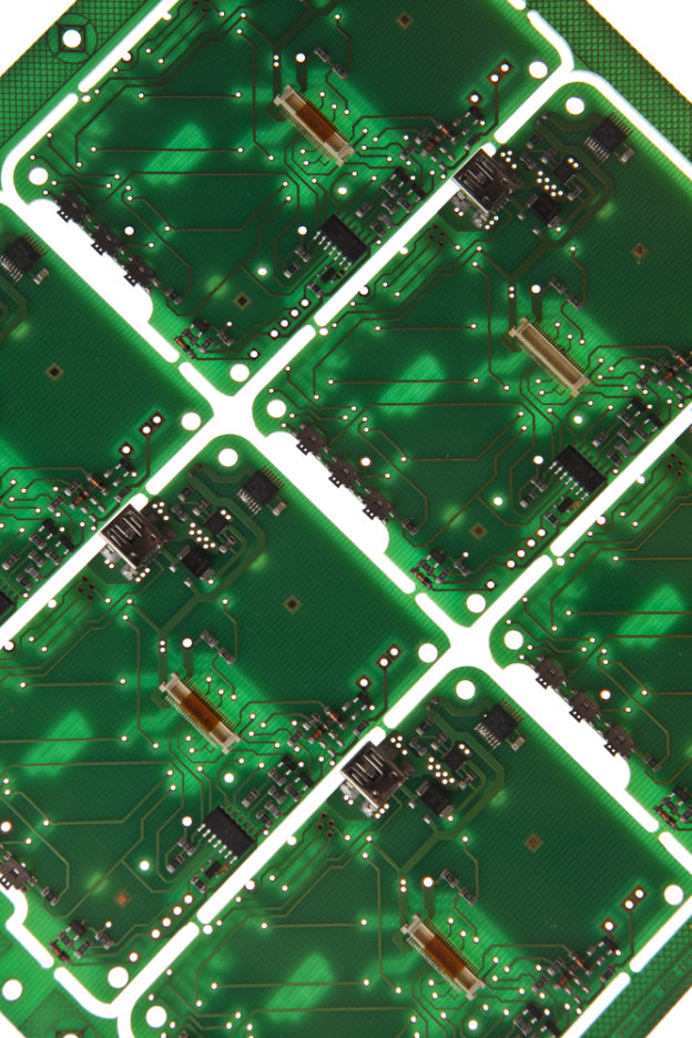
PCB – Stands for Printed Circuit Board. Printed circuit boards are found in every single device that uses computing and data. PCBs act as the “highway” in transferring data between components within a device.
THM – Stands for Through-Hole Mounting (also known as Thru-Hole Mounting). THM is an older assembly technology that mounts components on a PCB by drilling holes through the printed circuit board and placing component leads into the drilled holes. THM has largely been replaced by SMT assembly, though there are still some situations in which THM is preferred.
SMT – Stands for Surface Mount Technology. SMT was first introduced in the 1960s and rose to prominence in the 1980s. Today, it is the dominant form of PCB assembly. SMT does not require drilling holes through a printed circuit board. Its components are smaller than THM and can be placed on both sides of the PCB. This allows for a denser allotment of components and a more powerful PCB.
Substrate – The substrate is the actual board upon which wires and components are placed. It gives the PCB its structure and also insulates conductive parts. PCBs can be made from a variety of different substrates. All PCB substrates are non-conductive. Common substrate materials are: FR-4 (a fiberglass-epoxy laminate), Teflon, ceramics, specialized polymers
Traces – Traces are the things that electrically connect the connectors to the components. The most common material for the traces is copper. The copper layer of a PCB goes on top of the substrate. In double-sided PCBs, copper traces are placed on both sides of the PCB.
Soldermask – Have you ever wondered why almost all PCBs are green? This is the soldermask. This layer goes on top of the copper layer and functions to insulate the copper traces. It prevents the highly conductive copper traces from making contact with other metal components of the PCB.
While this is far from an exhaustive list of common terms used in the PCB industry, hopefully this guide will help you better understand and communicate with your printed circuit board manufacturer.
 Meizhou Ruiputuo Technology Co.,Ltd